Alchitry Cu FPGA Development Board Lattice iCE40 HX
Description
If you are not needing a lot of power to start your FPGA adventure, or are looking for a more economical option, the Alchitry Cu FPGA Development Board might be the perfect option for you! The Alchitry Cu is a "lighter" FPGA version than the Alchitry Au but still offers something completely unique. FPGAs, or Field-Programmable Gate Arrays, are an advanced development board type for engineers and hobbyists alike to experience the next step in programming with electronics. The Cu truly exemplifies the trend of more affordable and increasingly powerful FPGA boards arriving each year. This board is a fantastic starting point into the world of FPGAs and the heart of your next project. Finally, now that this board is built by SparkFun, we added a Qwiic connector for easy I2C integration!
The Alchitry Cu uses the Lattice iCE40 HX FPGA with 7680 logic cells and is supported by the open source tool chain Project IceStorm. The Cu possesses 79 IO pins with eight general purpose LEDs; a 100MHz on-board clock that can be manipulated internally by the FPGA; a USB-C connector to configure and power the board; and a USB to serial interface for data transfer.
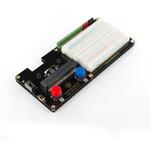
By adding stackable expansion boards similar to shields or HATs called "Elements," the Alchitry Cu is able to expand its own hardware capabilities by adding prototyping spaces, buttons, LEDs, and more!
The SparkFun Qwiic Connect System is an ecosystem of I2C sensors, actuators, shields and cables that make prototyping faster and less prone to error. All Qwiic-enabled boards use a common 1mm pitch, 4-pin JST connector. This reduces the amount of required PCB space, and polarized connections mean you can't hook it up wrong.
Get Started with our Learning FPGA Tutorials
Features
Lattice iCE40-HX8K FPGA - 7680 logic elements
79 IO pins(3.3V logic level)
USB-C to configure and power the board
Eight general purpose LEDs
One button(typically used as a reset)
100MHz on-board clock(can be multiplied internally by the FPGA)
Powered with 5V through USB-C port, 0.1" holes, or headers
USB to serial interface for data transfer(up to 12Mbaud)
Qwiic Connector
Dimensions of 65mm×45mm
Examples
First FPGA Project - Getting Fancy with PWM
External IO and Metastability
プログラミング/ロボティクス の新着商品
カテゴリ


